Testing turns assemblies into dependable products. We provide core quality control inspection and product-specific test development — from flying probe and functional test to burn-in and thermal cycling.

Testing turns assemblies into dependable products. Inspection and test are where workmanship becomes measurable and where early failures are caught before they reach your customer. Circuits Central provides core quality control testing as well as support for product-specific test procedures that improve confidence in reliability and function.
The biggest testing challenge most teams face isn’t choosing a test name — it’s turning functional requirements into a clear definition of “pass,” then building a repeatable process that doesn’t depend on individual knowledge. We help design, implement, and execute test strategies that scale with your product from prototype to production.
Test coverage should match risk, not just tradition. We help you select the tests that provide the most risk reduction for your specific product — not the most tests, and not the cheapest workaround. Then we implement them consistently and documentably across revisions.
AOI — Automated Optical Inspection
High-speed optical scanning detects solder defects, missing components, incorrect polarity, and placement errors across all visible surfaces.
X-Ray Inspection
Verifies hidden solder joints under BGAs, QFNs, and leadless packages. Detects bridging, voids, missing balls, and misalignment that optical inspection cannot reach.
Functional Testing
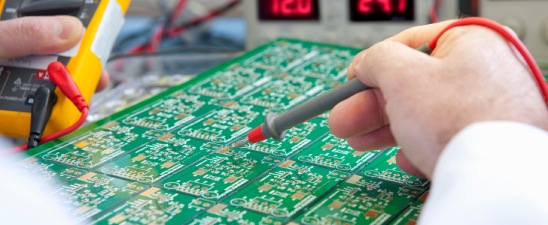
Validates the assembled board performs its intended functions under defined conditions using a purpose-built test setup. Catches integration issues that electrical testing alone misses.
JTAG / Boundary Scan
Uses IEEE 1149.1 architecture to test interconnects, load firmware, and validate digital logic without full physical probe access. Reduces fixture complexity for dense assemblies.
Flying Probe Testing
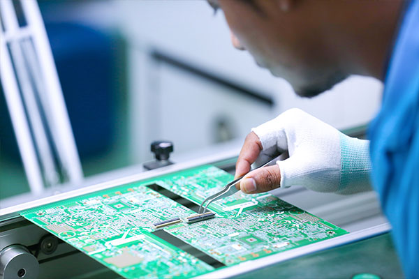
Fixtureless probing ideal for prototypes and low-volume builds. Tests continuity, shorts, and component values without requiring a dedicated test fixture design and build.
ESS, Burn-In & Thermal Cycling
Accelerated testing that exposes early-life failures and temperature-related weaknesses before product ships. Used when reliability screening is part of acceptance criteria.
| Test Method | Best For | Considerations |
|---|---|---|
| Flying Probe | Prototypes and low-volume — no fixture required, flexible for revisions | Coverage depends on test access points; slower than fixture-based methods at volume |
| ICT (In-Circuit Test) | Higher-volume production screening where fixture cost is justified | Fixture design and build lead time required; best for stable, mature designs |
| Functional Test | Validating end-to-end behavior including firmware and integration | Requires clear pass/fail definition, controlled inputs, and a known-good reference |
| JTAG / Boundary Scan | Dense digital assemblies with boundary-scan compatible devices | Requires device support and chain planning during design |
| ESS / Burn-In | Reliability screening and early-life failure identification | Must be defined carefully — unnecessary stress without clear objectives adds cost without insight |
Define the Risks
Identify the failure modes that matter most — power integrity, programming, RF performance, thermal stability, or specific functional paths. This drives the test selection, not convention.
Choose Measurable Criteria
Convert risk into measurable checks with explicit pass/fail thresholds. Ambiguous criteria create ambiguous results — clarity here saves debugging time later.
Confirm Test Access
Validate test point availability, connector access, boundary-scan chain, and fixture constraints before committing to a test method. DFT planning during design dramatically improves outcomes here.
Build and Validate
Run test procedures on early builds, compare against known-good references, and refine the procedure before committing to a production test plan.
Document and Control
Lock the test procedure to the product revision so results remain comparable across builds and revisions. Outputs include test logs, pass/fail summaries, and defect notes.
Test coverage improves significantly when planned during design. Simple decisions — reserving test pads, selecting accessible connectors, keeping programming headers consistent, and including JTAG chains where appropriate — save hours during bring-up and reduce fixture complexity in production. If you have constraints on enclosure access, power sequencing, or firmware loading, sharing those early helps define a test method that fits the product, not just the PCB.
In-circuit test uses a custom bed-of-nails fixture to test all targeted nodes simultaneously — high throughput, efficient at volume, but fixture design and build cost is significant. Flying probe uses movable probes without a fixture — more flexible, well-suited to prototypes and low-volume builds, but slower per board. The right choice depends on build volume, design stability, and how frequently the design is revised. Fixture investment makes sense once the design is stable and volumes justify it.
Trustindex verifies that the original source of the review is Google. Excellent PCB assembly services. We have had an excellent experience with Circuits Central. - Turn Around Time: Boards were always assembled on time including expedited projects with 24-hour TAT. - Customer Service: Customer service is fast to respond over email and resolve any outstanding issues very quickly. - Quality: Excellent assembly quality with no errors or issues including for complex projects. - Communication: Circuits Central made the jobs simple to submit. We didn't have to submit many files or prepare every last detail for them.Posted onTrustindex verifies that the original source of the review is Google. Circuits Central has been making our boards for over 25 years. They are a great company to work with.Posted onTrustindex verifies that the original source of the review is Google. Great customer service! Highly recommend the team at CCIPosted onTrustindex verifies that the original source of the review is Google. I've been using Circuits Central for over 10 years for all of our NPI projects. Workmanship is exceptional and deliveries are always on time. Many thanks to the Circuits Central team.Posted onTrustindex verifies that the original source of the review is Google. Excellent service and printed circuit assembly quality for 6 years so far, at a very reasonable price. Highly recommended!Posted onTrustindex verifies that the original source of the review is Google. Tailored Service Levels and Pricing. Excellent quality!
Please fill out the form below and we will get in touch with you to further discuss your needs.