Schematic & PCB Layout Design in Ontario

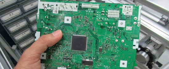
Design quality is manufactured quality. We provide schematic and PCB layout support with the added perspective of an experienced manufacturer — so layout decisions also support assembly, inspection, and scaling to production.

Full Design Support
DFM Built In
HSD/RF Capable
25+ Years Exp.
Printed circuit board over a schematic diagram
🇨🇦 Canadian-Owned & Operated
✅ 25+ Years Experience
📞 Direct Engineer Access
🔍 Full Traceability & Documentation

Schematic and PCB Layout Design

A PCB can be electrically correct and still be difficult to build, test, or scale. Circuits Central brings manufacturing perspective into the design process — so the decisions made during layout also support assembly, inspection, and future production.

Our schematic and PCB layout design services support hardware teams at any stage. Whether you have a complete architecture and need layout only, or you’re starting from product requirements and need full electrical design, we structure our engagement to fit your needs and remove bottlenecks before they affect schedule.

Manufacturing-aligned design: Because we also build and test PCBs, we understand what good documentation looks like from the assembler’s perspective. That experience reduces re-spins, prevents avoidable rework, and shortens the gap between first prototype and production-ready design.

Rows of printed circuit boards in a tray

Design Support Across the Full Development Cycle

Requirements & Block Diagrams

System-level definition, interface mapping, and block diagram development to establish design intent before schematic capture begins.
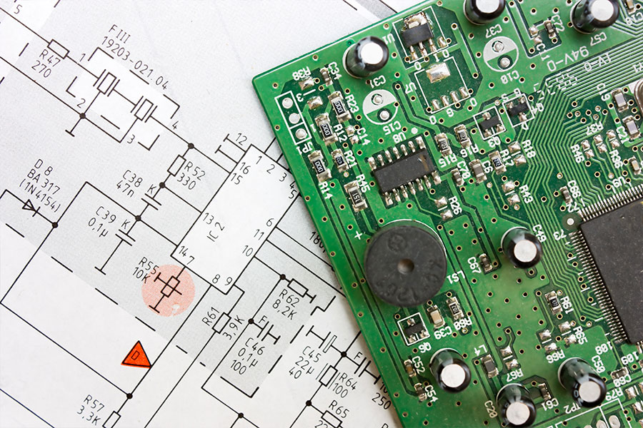
Schematic Capture

Structured schematic development with review for electrical correctness, net clarity, revision control, and design intent documentation.

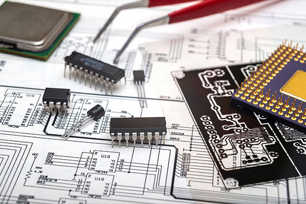
Footprint & Library Development

Land patterns, pin-1 marking, polarity indicators, and courtyard definitions that are consistent from schematic to the assembly drawing.

Placement, Routing & Constraints

Layout with performance, EMI risk reduction, and manufacturability in mind — constraint-driven from day one, not corrected in DRC at the end.

DFM & DFT Integration

Test point placement, boundary-scan planning, connector strategy, and assembly access reviews built into the design workflow.

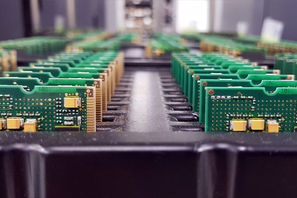
Production-Ready Deliverables

Gerbers or ODB++, drill files, pick-and-place, assembly drawings, BOM with alternates, and bring-up notes — a complete handoff package.

Component Selection

Why this matters at the design stage: A footprint error or single-source component costs relatively little to fix in schematic. The same issue costs significantly more to resolve after boards are fabricated, components are committed, and the first prototype comes back with a bring-up problem that traces back to a library entry.

Component Selection & Library Management

Component decisions made during schematic capture have consequences that persist through every build revision. A part selected without checking lifecycle status, package availability, or footprint tolerance can create sourcing bottlenecks, assembly friction, or redesign work that shows up months later — often at the worst moment in a product schedule. We address this upstream, during the design phase, not at the BOM review stage before a build.

In practice this means:

  • Lifecycle and availability checks at selection time— flagging parts that are end-of-life, last-time-buy, or single-sourced before they are designed in, not after the layout is locked
  • Approved alternate identification built into the component record so that the BOM arrives at assembly with substitution options already validated, not blank alternate fields that become sourcing emergencies
  • Footprint ownership and verification— every component in the library is tied to a specific land pattern with verified pad geometry, courtyard, paste aperture, and pin-1 callout. Footprints are not reused across package variants without review
  • Schematic symbol and footprint cross-check as part of design sign-off, confirming that pin assignments, polarity, and orientation are consistent from schematic to assembly drawing — a step that prevents a class of errors that don’t surface until bring-up
  • Common parts preference where functionally equivalent — reducing BOM line count, simplifying kitting, and improving availability resilience across product revisions
  • Package selection with assembly in mind— considering rework accessibility, inspection coverage, reflow constraints, and hand-solder feasibility where the design stage allows a choice

Design for Test (DFT) Planning

Test coverage during bring-up and in production is largely determined by decisions made during PCB layout — not by the test engineer after the board is built. Test points that weren’t placed, boundary-scan chains that weren’t planned, and programming connectors that weren’t sized for a pogo pin fixture are difficult or impossible to retrofit cleanly. We include DFT as a defined part of the layout process, not an afterthought.

DFT considerations we address during layout include:

  • Test point placement and accessibility— reserving dedicated test pads on critical nets (power rails, key signals, programming interfaces) with geometry and spacing compatible with bed-of-nails fixture or flying probe access
  • Boundary-scan chain planning— identifying JTAG-capable devices early, defining chain topology, and confirming that TDI/TDO routing and pull-up strategy support reliable chain integrity without requiring board rework
  • In-system programming (ISP) connector strategy— selecting connector type, pin count, and placement that supports production programming without requiring manual probe contact or custom adapters on every unit
  • Power sequencing documentation— capturing the intended startup sequence and any interlock conditions so that functional test procedures can be written against a known-good reference rather than reverse-engineered from board behaviour
  • Net naming discipline— consistent, meaningful net names in the schematic that carry through to the layout and appear in test reports, so that a failure on “TP23” traces back to a recognisable signal without decoding an arbitrary reference
  • Keepout coordination for test fixtures— identifying component height constraints and keepout zones near high-density or tall components that would prevent fixture probes from reaching target pads

For teams that already have an ICT fixture, a functional test script, or a defined bring-up procedure, we review those requirements before layout begins so that test access is planned to match — not approximated and corrected after the fact.

Design for Test Planning

Engagement Model Options

Selecting the right engagement depends on how much design is already complete and what your schedule looks like. Common options include:
Engagement Best Suited For Considerations
DFM Review & Feedback Designs near release — targeted improvements before fabrication Best when design is largely complete; cannot replace missing requirements
Layout Only Complete schematic provided — focused on placement, routing, and outputs Requires complete schematic and library clarity before starting
Full Design Requirements to production-ready layout under one team Up-front discovery phase is essential; missing requirements cause late changes
Design + Prototype Build Short feedback loop between design intent and build results Requires coordinated schedule for sourcing, assembly, and bring-up support
Holding a green printed circuit board.

Deliverables That Reduce Ambiguity

A complete handoff package lets fabrication and assembly move without unnecessary back-and-forth. Our standard deliverables include schematic PDFs and source files, PCB layout database and fabrication outputs (Gerber or ODB++), assembly outputs (pick-and-place, assembly drawings with polarity callouts), a BOM with manufacturer part numbers and approved alternates, and bring-up notes tied to the product revision. We validate placement outputs with a CAM viewer before release — origin and rotation convention mismatches are a known cause of uniform placement offsets and are preventable with a pre-flight check.

Frequently Asked Questions

A typical engagement starts with a review of requirements and functional intent, followed by schematic capture, component selection, and early DFM input. PCB layout then addresses placement strategy, signal integrity and routing constraints, power distribution, and design-for-test considerations. The process concludes with a thorough design review, generation of final fabrication and assembly outputs, and change control documentation so that revisions remain traceable. The goal is an output package that goes to fabrication and assembly without ambiguity.
A DFM review at Circuits Central typically evaluates Gerber files, the BOM, pick-and-place data, and assembly drawings against manufacturability constraints such as component clearances, pad geometry, thermal relief, panelization, and testability. Identifying issues at this stage — before boards are fabricated or components are committed — reduces rework, shortens the path to a clean first build, and improves long-term yield. DFM feedback is most valuable when it happens early in the design cycle rather than after layout is locked.
We flag lifecycle status — end-of-life, last-time-buy, single-source, and constrained availability — at the component selection stage, before a part is designed in. For each flagged component we identify at least one validated alternate and document it in the component record so it carries forward into every BOM revision. This is significantly cheaper to address during schematic than at the quoting stage of a production build, when re-spinning the layout may be the only option if the primary part is unavailable.
DFT is addressed as a defined part of the layout process, not added after routing is complete. This includes test point placement and geometry compatible with flying probe or bed-of-nails access, boundary-scan chain planning for JTAG-capable devices, in-system programming connector selection and placement, power sequencing documentation, and keepout coordination near tall components that would block fixture access. If you have an existing test fixture, ICT setup, or bring-up procedure, we review those requirements before layout begins so that access is planned to match rather than approximated.
We offer both. Some projects arrive with a complete, verified schematic and need layout only — we support that efficiently. Others need end-to-end support from requirements and block diagrams through verified layout and a full production package. The engagement is structured to fit where your design actually is, not a fixed process that assumes you’re starting from scratch.
Repeatability comes from controlled revisions, consistent sourcing decisions, clear assembly notes, and defined inspection or test expectations — established from the first build rather than retrofitted after problems emerge. When these elements are in place early, prototype results stay meaningful and comparable across build cycles, rework is easier to isolate and attribute, and the transition into pilot runs or production becomes significantly smoother.
A standard deliverable package includes schematic PDFs and native source files, PCB layout database and fabrication outputs (Gerber RS-274X or ODB++), drill files with stack-up notes, assembly outputs (pick-and-place with explicit origin and rotation convention, assembly drawing with polarity and pin-1 callouts), a BOM with manufacturer part numbers and approved alternates, and bring-up notes when product-specific testing is in scope. We validate placement outputs with a CAM viewer before release — origin convention mismatches between the placement file and fabrication data are a preventable source of uniform placement offsets.

Request Information

Let's Start the Conversation

Please fill out the form below and we will get in touch with you to further discuss your needs.

1 Quotation Specification*
Quotation Type
2 Quantity
3 Upload
Upload file
Please choose a "jpeg", "jpg", "png", "doc", "pdf", "gif", "docx", "zip", "xls", "xlsx" file.
4 Contact Information
5 Lastly, how did you hear of us?
Back