3D-Printed Circuit Boards: The Future Is Here
Technology has been changing the face of business, including manufacturing and engineering. With the development of 3D printing, how we design products has been revolutionalized. Modern 3D printing has made creating items, such as circuit board prototyping, more cost-effective and efficient.
Although the industry is still developing, 3D printed circuit boards can improve prototyping cycles while advancing production precision.
What are 3D Printed Circuit Boards?
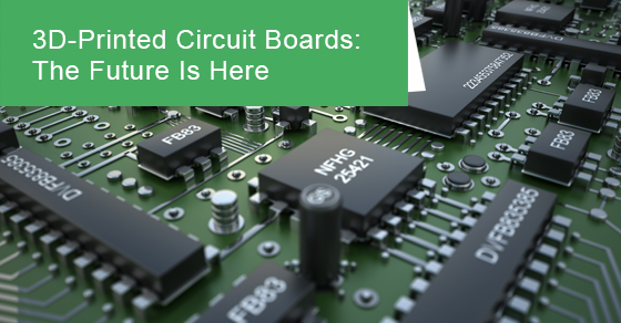
Printed circuit boards are essential electrical components for your phone and computer. Manufacturers can use 3D printed circuit boards to develop complex wiring and organize it in a small, compact space. The advantage of 3D printing is that it takes less time and costs less money than traditional printed circuit boards.
Benefits of 3D Printed Circuit Boards
Easier to Create
With a 3D printed circuit board, designers don’t need to spend the time etching out a printed circuit board to create a prototype.
Unique Designs
The innovation of 3D printing means there is no limit to a manufacturer’s shape or design of a 3D printed circuit board. These circuit boards will be able to take different forms to fit onto any type of circuit carrier. And they’ll retain the vital electrical components needed. In other words, they can be as small or as large as the project calls for.
Efficiency
Creating circuit boards with a 3D printing process means less wasted materials. The printing process is so refined that it only uses the necessary amount of material. Moreover, by using a computerized printing method, human error will be further reduced for circuit board design and printing.
Green
With less wasted materials, 3D printed circuit boards can be made using any material, including low-cost, recyclable material.
Drawbacks of 3D printed circuit boards
While 3D print has advantages for printed circuit boards, there are still some drawbacks to what can be accomplished. These include:
Lack of Software Support
The support available to help understand and work with CAD programs needed to design and create circuit boards is pretty limited. This means you’ll need to have a strong background in circuit board design to be able to start building.
Material Conductivity
The material used in the hollow trace method is not as conductive as metal. The electrical resistance of the material complicates the design process.
How 3D Printed Circuit Boards are Created
The process of creating a 3D printed circuit board is intriguing. There are two main methods used. These are:
1. Conductive filament
The 3D printer lays down conductive filament along pre-created tracks designed using CAD software with the conductive filament process. This creates a pattern of lines so that the item resembles a traditional printed circuit board. This method allows for various layers of circuitry to be used. Designers can also include other forms.
2. Hollow traces
In this method, the 3D printer produces hollow traces that can be filled in with conductive material at another time. This material will be either electric paint or conductive epoxy. However, this method does not allow for complex designs with various components.
Their budget and expertise will determine the method that a designer chooses to use. The conductive filament technique is less expensive than the hollow traces approach. However, the first process can be more complex.
Future of 3D Printed Circuit Boards
While the concept of 3D printed circuit boards is still just for prototyping, technology can move quickly. Currently, engineers use 3D printed circuit boards to test their designs. However, the possibilities are exciting as 3D printing will reduce costs and speed up turnaround times. It could help spur innovation in the industry, leading to more creative designs and products.
There have been some possible predictions of how 3D printed circuit boards could be used, such as:
Board Cameras
Cameras can be mounted directly on a circuit board. They are fully functioning and capable of taking videos and photos. They have a lens, aperture, and image sensor but are just the size of a quarter. The consumer advantage is that cameras this small could fit on nearly any device.
Consider the ways that a board camera could be used:
Consumer electronics - image if any device had a camera installed. Smartphones and tablet cameras have been commonplace and very popular options for board cameras. As demand continues for these devices, manufacturers will compete to make them smaller and more powerful.
Medical instruments - board cameras have been used to assist medical professionals in conducting non-invasive and minimally invasive procedures. They’ve been valuable instruments that can improve the accuracy of diagnosis. Ways that these board cameras have been used include pills that patients can swallow so physicians can diagnose digestive problems and spot any other troubles. Surgeons have also been employing board cameras as wearable tools.
Surveillance - the tiny size of board cameras makes them an ideal surveillance method. They can be conveniently hidden in various places and record videos to assist law enforcement officers in capturing criminals. Homeowners and businesses can also use them to protect their property.
There are many other ways that board cameras can be used. As the technology continues to develop, we’ll likely see smaller and more durable board cameras.
Printed Electronics
3D printed circuit boards are changing the way electronics are designed and created. Using 3D printing technology means developers could create and print circuit boards in any shape. It allows for more creativity and innovation in the electronics industry.
For more information about 3D printed circuit boards, call Circuits Central at 1-800-602-7264 or contact us here.