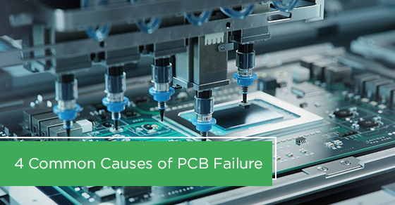
4 Common Causes of PCB Failure
These days, all kinds of electronic devices have printed circuit boards (PCBs) as central components within them. PCBs are necessary to connect various components to one another via a complex array of circuits and copper conductors.
There are many different design types of PCBs, which vary depending on factors related to the kind of device they are to be used in. Although PCBs are often meticulously designed and carefully manufactured, they are not indestructible and can occasionally fail.
Even though several types of issues can lead to PCB failure, the end result is always the same: the PCB reaches a point where it no longer functions properly. Of course, if a PCB stops functioning, the device it is used in will also be unable to operate.
Since PCBs are used in many incredibly important electronic devices, such as medical equipment, airplanes, and satellites, it is crucial that potential causes for failure can be identified so that necessary steps can be taken to prevent such failure if possible.
What are the most common reasons for PCB failure?
Due to the fact that PCBs have complex designs and manufacturing processes, there are numerous opportunities for failure to take place. Occasionally, PCB failure can stem from design oversights or measurements that are slightly off during such processes.
Sometimes, even when the design is flawless, major errors can also happen during the manufacturing process, such as drilling errors or over-etching. The following are some of the most common reasons for a PCB to fail:
1. Plating voids
All printed circuit boards have copper-coated holes, which are known as plated through-holes. The function of these holes is to allow electricity to flow from one side of the board to the other.
To create through-holes, a process known as deposition takes place. This involves drilling holes all the way through the board and adding a layer of electroless copper coating to the surface of the material and the walls of the holes. Unfortunately, sometimes, the material does not coat evenly during the deposition process, resulting in gaps or holes in the plating, known as plating voids.
Plating voids may pose problems since imperfect through-holes can potentially prevent electrical currents from passing through them. Most of the time, the reason behind plating voids is either material contamination, air bubbles, inadequate hole cleaning, or insufficient catalyzation of the copper.
Cleaning the material thoroughly after drilling is the best way to avoid the first three issues, while closely following standard catalyzation procedures can eliminate the fourth one.
2. Insufficient copper-to-edge clearance
Copper is an active component used in the manufacturing of PCBs. Unfortunately, this material is rather soft and can easily become corroded. For this reason, it is often covered with other materials to prevent such corrosion from happening.
However, when the copper is too close to the edge of the PCB and the PCB is trimmed, some of this coating material may also be unintentionally trimmed, which exposes the copper underneath. If this happens, there are a number of issues that can occur related to the PCBs’ functionality.
One major issue is that it becomes possible for the exposed copper planes to simultaneously make contact with a conductive material, which would cause a short to occur. Of course, the copper also becomes vulnerable to corrosion once again since it is exposed. To avoid such problems, it is necessary to ensure that PCBs are always designed to have at least some space between the copper and the edge of the board.
If you are uncertain about whether the current will flow from one point to another in your PCB, you can always perform a high potential test in Toronto to check for good isolation. Performing a high potential test will help you to ensure that no such current flows are possible.
3. Slivers
During the PCB manufacturing process, when the etching is performed, narrow wedges of copper or solder mask can be formed, resulting in various problems. If an overly long, thin copper feature is etched away and detaches before fully dissolving, it can float around in the chemical bath, potentially becoming attached to another board and creating an unintended connection.
Similar slivers can also be formed when sections of the PCB are cut either too narrowly or too deeply. This causes part of the material to peel back or detach, connecting to other copper pieces or exposing copper plating that should be covered, and leading to either a short or copper corrosion and, ultimately, reducing the lifespan of the PCB.
For the most part, these kinds of slivers can be avoided by designing sections with minimum widths.
4. Acid traps
When there are acute angles in a circuit, they are known as “acid traps”. They trap acid during the PCB etching process, which allows it to build up in the angle’s nook and eat away more than it should, compromising connections and potentially leading to bigger issues.
Most of the time, PCB designers are trained to avoid using acute angles in the design of a circuit. However, due to human error or improper settings adjustments in design software programs, they can still occasionally be included. Thus, it is always necessary to double-check PCB design work and have the manufacturer perform a DFM (design for manufacturability) check just to be sure.
How Circuits Central Can Help You Avoid PCB Failure
Through various means, such as high potential tests in Toronto, Circuits Central can help you avoid the inconvenient and potentially dangerous problem of PCB failure. If you have already designed and manufactured a PCB, but you suspect it may be susceptible to failure, we can test it using advanced methods and technologies to find exactly where the issues are so that the quality can be improved and your time-to-market can be reduced.
Our team of experienced PCB design and manufacturing experts will be able to develop, implement, and execute testing specifications that are custom-tailored to your PCB to ensure that every possible issue is detected.
If you want to avoid dealing with potential PCB failure in the first place, you may want to consider coming to us to have your PCB designed and manufactured from beginning to end, as we can guarantee top-quality work.
Our engineers will follow the highest possible standards of quality control throughout the process of designing and constructing your PCB, and will work closely with you to ensure that all of your needs are met. We perform rigorous in-house testing all throughout the process to ensure that your PCB will not move on from one step to the next before we are certain that there are no problems present.
For more information about how we can help test your PCB for potential defects or to learn more about our PCB design and manufacturing services, call Circuits Central at 1 (888) 602-7264 or contact us here.