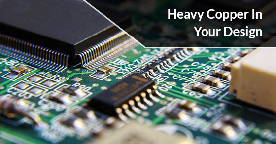
5 Things To Consider When Using Heavy Copper In Your Design
Many printed circuit board manufacturers are using heavy copper in their prototype productions. If you plan on doing the same, here are five things to consider when using heavy copper in your PCB design.
- The Etching Process Has Improved
Heavy copper PCBs were once structured through a complex etching process. This process left uneven traces and inaccurate undercutting. Nowadays, when heavy copper is used in prototype productions, the etching process is more specialized and sound. Through technological advances, heavy copper features can now be formed by combining high-speed plating and differential etching. This process produces easy undercutting and even sidewalls.
- Heat Rise and Current Flow Are Analogous
Heavy copper PCBs are capable of carrying current. However, how much current will vary depending on the thickness and width of the copper and the highest temperature rise the PCB can withstand. To determine the maximum current a trace can carry safely, you need to figure out the associated heat rise with the applied current.
- The Benefits to Your Prototype Productions Are Numerous
When you use heavy copper for your PCB you get increased endurance to thermal strains and increased mechanical strength at the connector sites. In addition, when you use heavy copper you avoid circuit failure at high temperature, and the copper plated vias are able to carry higher current throughout the board to move heat to an external heatsink.
- Use Heavy Copper for Traces and Pads
Lighter copper will fail when it’s faced with lower mechanical and thermal stress. For traces and pads, use a heavier copper instead, so that the dielectric breakdown and voltage rating of the PCB doesn’t diminish.
- Military Applications Rely on Heavy Copper
Although you may not be creating prototype productions for the Canadian military, you can mimic their process. Traditionally, high current circuits are created by adding duplicate parallel layers of 3 or 4 oz copper to allow the layers to evenly share the current. However, current sharing isn’t always ideal, depending on the application.
Instead, with heavy copper in the high current circuits, combined with thicker copper plating in the vias (plate it through holes), you eliminate the need to adjoin duplicate parallel layers. In doing so, temperature rises caused by losses in the boards can easily be calculated, and the thick copper plating in the holes curtails failures that are linked to thermal stress.
For more information about prototype productions using heavy copper, please contact Circuits Central.