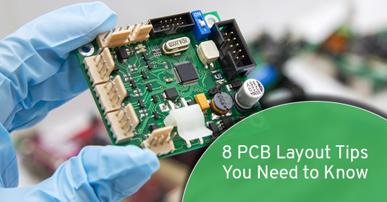
8 PCB Layout Tips You Need to Know
The design and development process of a printed circuit board (PCB) is divided into several steps. Each step is essential for creating a circuit that can perform necessary operations in a short amount of time.
First, you must select the materials and physical structure (layering and stacking) of your PCB. After that, it is necessary to position the components according to their distribution among the layers and route the traces.
We will explain that last point further and offer a few tips that will help you simplify routing while avoiding some common pitfalls. If you follow these tips, routing can be one of the most delicate and rewarding stages of PCB design. For this reason, experienced professional PCB designers are often referred to as artists.
PCBs are everywhere we turn. In fact, most of us are never more than a few metres from one. They are in your smartwatch, your laptop, and mobile devices. There is probably not a day that goes by that you do not use a PCB! That is why PCB design is vital today. In this post, we have included our top 8 layout tips that are crucial to know, each of which discusses important elements of PCB design.
1. Node location is critical
One of the most important aspects of PCB design is ensuring the accessibility of nodes. Doing so can assist you with both your design and testing issues. Tests will be much harder if you cannot access the nodes, regardless of how many of them you are using. Probes must also be easy to access for successful testing to occur.
2. Space matters
Circuit boards can now contain more components per square centimetre than ever before. That is good news for consumers. The more components there are on one board, the more functional and useful a device is to its users. It can be challenging for designers to determine the best option for users.
Boards with more components become cramped as those components are added. Never underestimate the importance of component spacing. There will be no places to route the wires without the appropriate space. Most components also produce heat, which presents a bigger problem when boards are more densely packed.
However, choosing the right material to construct your board could solve this issue. Use a board material designed to withstand high temperatures rather than a material like FR-4.
3. Heat-related issues
Problems related to heat are perpetual when it comes to PCB design. However, these matters can be dealt with. You can shield surface-mount components from heat if you add extra copper. When you create additional surface area, a portion of the PCB is effectively converted into a heatsink.
4. Take note of how things are arranged
Occasionally, your design will require more than a mere rotation of the components. Sometimes, it is useful to have a more strategic approach regarding the placement of your PCB’s various components.
- Cascaded components play a crucial role in a lot of PCB design options. However, properly arranging cascaded components can be a challenge. Keep them close together and arrange them in a sequence on the board. That will eliminate the hassle of routing traces in multiple directions across the board.
- Combine various components whenever possible. It is unnecessary to have multiple small resistors when a single higher resistance resistor is adequate. Simplifying your design will give you more space for other components and traces.
- Figure out which components must be attached via a connector. The connector will be located close to or right on the edge of your PCB. Therefore, you should position all these components as close to that area as possible. That way, all functions in the chain will cascade away from that point in an organized sequence.
5. Create space
Many PCB designers struggle to route traces between PCB components. Especially when the board is small, there may be problems wherever you put them. Have you ever experienced this?
Do not worry! You can solve this common problem by arranging the components in a way that will allow you to route traces between them directly while maximizing the board's surface area. Making this work may require time and effort, but the results will be well worth it.
6. Overcrowding the board
Have you dealt with a board that is seemingly unroutable? One way to fix that is to reduce the size of your components. Smaller footprints give copper traces more room to pass between the components. You can maintain proper spacing more easily with smaller components. That way, you can avoid overcrowding and the compounding problems that come from stacking components too close together.
Consider using ball grid array components rather than quad flat package components. Unfortunately, one drawback here that is important to note is that repairing smaller components can be more challenging.
7. Go denser
If you are having difficulty designing PCBs, your main problem may be finding the space required for traces, vias, and clearances. Densification can help with that. Creating traces, vias, and clearances that are very dense with HDI will still allow your PCB to perform excellently. When it comes to high-current and high-voltage design, you have to pay attention to controlled impedance routing, differential pairs, as well as creepage, clearance, and width.
8. Keep noise to a minimum
Certain traces can be affected by signal noise. If you place traces carrying high-frequency signals too closely together, it may cause the signals to couple, ratcheting up the noise and posing problems for traces without any noise. To avoid this problem, you should keep noisy digital traces separate from analog traces.
For more information about PCB design layout and PCB Assembly, call Circuits Central at 1 (888) 821-7746 or contact us here.