Dye and Pry Testing: Advantages and Disadvantages
Even the tiniest details are of extreme importance when manufacturing printed circuit boards because if one small aspect of the circuit is off, the whole thing may not work.
A device that is not working can be incredibly frustrating, especially because isolating the problem causing the malfunction can be an extensive, time-consuming matter. Fortunately, a testing method called dye and pry testing can help shorten that process and make it much easier for you to identify where the issue or issues lie.
Dye and pry testing is a failure analysis technique specifically for testing solder joints on PCBs, as it can identify unique defects, including cracks, "head-in-pillow" defects, and other joint separations. Dye and dry testing can also reveal hidden discontinuities beneath any SMT components you are dealing with.
How is this kind of testing performed?
The dye and dry process starts by using a specialized saw blade engineered for precision circuit board cutting to excise a decent-sized sample of the board that contains the target feature you want to test.
Following the excision, the model must be submitted in a low-viscosity special dye inside a vacuum chamber, immersing it entirely so that every component is completely covered.
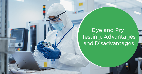
After that, the sample must be baked in a moisture removal oven until it dries completely and then fully disassembled by a puller assembler. After the parts are all separated, they can be carefully examined under a microscope, looking for any defects or anomalies introduced by the testing process.
What are the advantages of a dye and pry test?
There are many reasons why dye and pry testing is such a popular PCB testing method. There are many benefits to using this approach over others, such as X-Ray analytical techniques. The following are the main advantages of dye and pry testing that makes it worthwhile:
One of the main advantages of dye and pry testing is that it beats out any other testing methods in its capacity to cover an entire BGA unit with ease and precision and outperforms other methods in terms of its detection capabilities.
In addition, dye and pry testing is the most cost-effective option available. It tests all the joints on a BGA simultaneously, making the testing process quick and efficient and allowing you to cover a ton of ground simultaneously.
Dye and pry testing can also locate very fine cracks and cratering that would otherwise be impossible to find even with the use of robust X-Ray systems. On top of that, this kind of testing has a significant amount of documentation and compliance standards available to back it up, which should help guarantee your confidence in it.
What are the disadvantages of a dye and pry test?
Although dye and pry testing are among the most widely accepted techniques for characterizing solder joint quality defects in PCBs, this method has some disadvantages. The following are some of the main disadvantages that are worth considering before using dye and pry testing on your PCBs:
One of the significant downsides to dye and pry testing is that it is destructive, meaning it typically is not possible to reanalyze the components with other methods after they have gone through the dying and prying since they may receive damage beyond repair.
In addition, dye and pry testing is limited to detecting surface flaws. Testing on rough surfaces could lead to false indications due to difficulty removing excess penetrants. Proper training and handling are necessary since spraying the penetrant could lead to skin irritation if misused.
Once you make it to the final step of the testing process, extensive expertise is required to optimize the sample preparation for an accurate and complete analysis.
How Circuits Central Can Help with Your Dye and Pry Testing
If you want to test your BGA devices thoroughly, nothing can compare to the dye and pry method. Yet, this process is complex and requires a vast amount of specialized tools and expertise. Fortunately, even without having access to those tools or without expertise, you can still get dye and pry testing done, as Circuits Central can be of assistance when it comes to dye and pry in Waterloo.
We have the skills and the necessary equipment to provide you with top-notch dye and pry testing on any BGA devices you need to have tested.
At Circuits Central, we understand the true value of post-production testing, as it is the best way to ensure that PCBs are performing as expected. That is why we are incredibly stringent and rigorous with our testing protocols, including our dye and pry procedures.
Our team members will execute thorough testing to ensure that your products' reliability and functionality meet your specifications while also meeting and exceeding industry standards.
Suppose you are interested in trying out other testing methods to guarantee the quality of your products. In that case, we also have the facilities and the capabilities to perform a variety of different tests that each come with their own benefits, including functional testing, JTAG testing, In-Circuit testing, environmental stress testing, single-sided flying probe testing, double-sided flying probe testing, burn-in, and thermal cycling.
For more information about dye and pry testing or to learn more about our other PCB testing services, call Circuits Central at 1-(888) 602-7264 or email us at info@circuits-central.com.