Electronic Manufacturing of Printed Circuit Boards
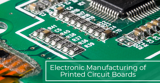
All major electronic components have a printed circuit board (PCB), which serves as the backbone of each component. Even rather rudimentary devices, such as calculators and digital clocks, have printed circuit boards, and virtually all computational electronic devices have one too. The purpose of a printed circuit board is to route electrical signals through an electronic device. By doing so, the mechanical circuit, as well as the electrical circuit requirements of the device, will be adhered to. Here, we break down the steps involved in the electronic manufacturing of printed circuit boards.
Output and Design
To begin, the designer will use state-of-the-art PCB design software in order to create the proper PCB layout for compatibility purposes. Some popular examples of PCB design software that designers may use include Eagle, Pads, and Altium Designer. The contract manufacturer will then need to approve of the PCB design so that production can commence. Next, the designer will need to export the design according to the format that the contract manufacturer deems acceptable. Currently, the most popular program for design exporting is known as extended Gerber, which is sometimes referred to as IX274X.
Moreover, in order to reduce the probability of errors, the software will perform an oversight algorithm on the PCB design. The designer will also perform quality control analysis in regards to the hole size, hole and trace spacing, board edge spacing, and track width. Once a meticulous overview of the PCB file is complete, it is then sent to a PC Board House so that production may begin.
The Filming Process
Next, the manufacturer will perform a design for manufacturing (DFM) check. Photo films of the PCB will be made via a plotter, which is a special type of printer. The photo films will be used to image the PCBs, and the plotters provide very high quality and precise printing technology in order to generate a detailed film of the PCB design. The final product will consist of a black photo negative of the PCB in a plastic sheet.
Copper Foiling
In the third step, the goal is to print the figure found on the photo film onto an actual copper foil. In other words, this step consists of actually making the PCB itself. A PCB—in its basic form—consists of a laminate board with a glass fiber and epoxy resin core. The laminate material is designed to house the copper that serves as the structure for the PCB. As for the substrate material, it is designed to provide a dust resistant and sturdy starting point for the PCB.
In any event, the copper is pre-bonded on both the front and the back, and is done by whittling away the copper on both sides. Furthermore, as cleanliness is paramount in this step, the laminate is passed through a decontamination environment. Even a single speck of dust can suffice to create a short or open circuit, so it is imperative that no dust particles make their way onto the laminate during the copper foiling process.
Removing Excess Copper
The fortified layer, termed “photo resist”, will protect the copper that is housed within its walls. In this step, the goal is to remove any excess copper by using a copper solvent solution. The amount of solution required will vary from one PCB to another, as not all copper boards are equivalent. The hardened resistance that protects the desired copper will also need to be washed off using a different solvent product. The end result, when performed correctly, is that the PCB will glisten, and only the copper substrate that is needed for the PCB to function optimally will remain.
Layer Alignment
Here, alignment punches will be needed to make sure that all the layers line up as they should. The inner layers will be aligned to their outer counterparts via the registration holes. After the layers are cleaned and ready to go, the technician in charge will place the layers into an optical punch, which is a top-of-the-line piece of machinery that allows for an accurate correspondence so that the holes are punched precisely.
Moreover, in order to confirm that there are no defects present, a second machine is used to perform an optical inspection of the panels in question. If the second machine detects an inconsistency, then the data will be generated on a screen for the technician to assess. Once the layers pass the last inspection process, the product is moved to the final stages of production.
Layering, Bonding, and Drilling
In this stage, the actual circuit board will take shape. The outer layers will need to be bonded to the substrate. The bonding process takes place on a steel table with metal clamps. A pre-impregnated (prepreg) layer is then placed over the alignment basin. The substrate layer will need to be placed over the prepreg before the copper sheet is placed. A copper press plate and aluminum foil are included to complete the stack before it is prepared for pressing.
After the layers are molded together in a PCB “sandwich” of sorts, the restraining pins are extracted and the top pressure plates are thrown away. This stage consists of drilling. Holes are bored into the stack board. In addition, in order to determine where to precisely drill the holes, an X-ray locater is used. To continue reading about the steps involved in PCB manufacturing, please click here.
Circuits Central
If you require the services of an electronic manufacturing services company, then we can help. Circuits Central is a cutting-edge electronics manufacturing services company. If you would like to learn more about our electronic manufacturing services company, then please visit our website or give us a call at 1-888-602-7264.

