
PCB CAD Design for Manufacturing Guidelines: Trace Routing and Solder Joints
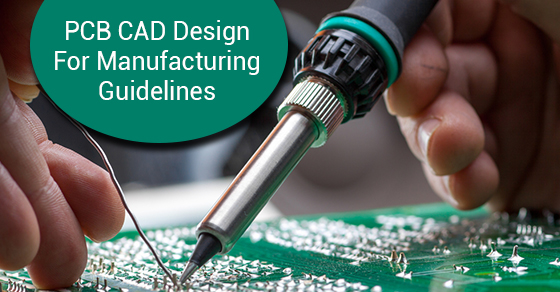
When a printed circuit board is manufactured, it's important that all the parts are executed perfectly. If even one part of the design is flawed, the entire thing will cease to function at best. At worst, the piece might pose a hazard to people. One bad solder can destroy an entire board. But you can adhere to design for manufacturing rules, otherwise known as DFM rules, to keep your solder joints uniform and efficient.
DFM rules cover obvious things like safe handling of your circuit boards and uniformity among your soldering. But there's another place where they can help: the way you choose to route traces regarding your PCB directly affects potential solder problems, and DFM rules can give you guidance.
This post will dissect the different ways that trace routing has the potential to cause problems so that you can avoid these scenarios in the future.
Acute Angle Traces
One potential problem lies in acute angle traces. This circumstance isn't guaranteed to lead to solder problems, but it is noted in DFM guidelines.
In traces, an acute angle describes a trace whose corner is larger than 90 degrees. This corner causes the trace to angle back on itself. When a wedge is created, this wedge might trap acidic chemicals when the board is fabricated. The trapped chemicals aren't always cleaned the way they should be, and they'll continue to eat at the trace until it breaks or begins to cause sporadic connections.
Tombstoning
"Tombstoning" refers to the effect of a two-pin part being stood up on one of its pads when soldering occurs. This generally happens because the two pads have a heating imbalance when solder reflow occurs. When one side melts before the other, it pulls the piece toward that side instead of holding it flat, which causes the "tombstone" effect.
Heating imbalances can be caused by a myriad of different factors. One of these is the use of different trace sizes on the pads. When the trace is wider, the pad will take longer to heat. If one pad has a wide trace, and one pad has a narrow trace, there will be a heating imbalance during soldiering. You'll then see the tombstone effect.
Sometimes electrical engineering plans require power traces that are too wide to be soldered by the manufacturer. Because of this, PCB guidelines recommend minimum and maximum widths for the traces used on different types of parts. However, this isn't guaranteed to solve the problem. To fix the issue, you need to balance your manufacturing and electrical engineering requirements so that the two can work in harmony.
Cold Joints When Soldering
When you route thick traces, you might accidentally create a cold solder joint. This is a joint in which solder has not been correctly reflowed, and therefore the solder does not make an ideal connection. Alternatively, the solder might have pulled back from the connection entirely. This occurs when you route a thick trace with a pad, and the trace size pulls the solder from the pad when the solder needs to be placed on the pad to make connections.
The main solution to this problem is only to use trace widths that are smaller in size than the pad. Certain DFM guidelines make a recommendation that you don't use a trace with a wider width than 0.010 mils. That said, you'll need to balance the manufacturing and electrical engineering components of your design to find a harmony that works best for the project.
Use the PCB and DFM Guidelines
PCB guidelines encompass much more than trace routing guidelines. In the same vein, DFM guidelines can help you to use the correct placement techniques for your components, standardize your footprint sizes, and accurately render other pieces of the overall design. These guidelines are implemented to keep your design from being manufactured with errors.
When circuit boards are free of errors during the manufacturing process, this is a sign that the design is good and solid. You've taken care to put thought into the design components and the ways they work together.
You might use software for your PCB manufacturing designs. Design software has the kind of advanced routing capabilities that you'll need to troubleshoot potential manufacturing problems. If you're a designer, using PCB manufacturing software will help you deliver a sound and DFM compliant design to your manufacturer on the first try. It streamlines the process and helps with your overall efficiency.
Ensuring Your Manufacturing Process Is Compliant With DFM Regulations
Circuits Central is a company which provides solutions to electronics manufacturing problems. Our solutions can be applied to the pre-manufacturing design and refining process, the actual process of manufacturing, and the post-manufacturing distribution process.
Our team of designers and engineers can help you with your circuit board designs. If you're stuck, a consultation can help you to troubleshoot the problems you're having. Our engineers are also well versed in DFM and PCB compliance, and they can give you tips to help you streamline your process more efficiently.
When you're troubleshooting your potential problems, Circuits Central provides the following services:
- Designs made from scratch for electronic circuits and circuit boards, created with cutting-edge software and experienced methods
- Huge amounts of detail throughout the entire design process
- Engineering expertise provided by an engineering team with years of experience
- Analysis of problematic designs and suggestions for solutions and upgrades
- Custom creation of a components library
- Firmware development
- Digitization of designs
- DFx consultations
If you've already completed your design, the following manufacturing services are available:
- Twenty-four hour production services
- Modification, upgrade, and rework services
- PCB repairs
- Supply chain planning
- Rapid prototyping
- Environmental stress tests
- Documentation of production
- Certifications of regulations
To get in touch and find out more about our solutions, call us today at 888-821-7746 or contact us here.


