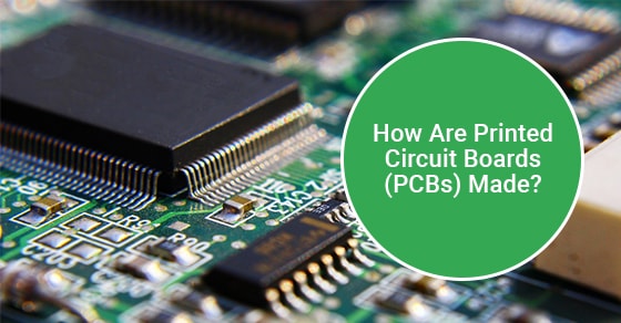
How Are Printed Circuit Boards (PCBs) Made?
When it comes to PCB manufacturing, there are over a dozen intricate and nuanced steps that must transpire in order for everything to work smoothly. PCBs also serve as the backbone of all major electronics in the industry, so PCB manufacturing is something that should never be taken lightly. From calculators and digital clocks to top-of-the-line computational electronics, PCB manufacturing is integral to the fabrication of various electronic devices. Here, we will discuss the various steps that are involved in PCB manufacturing.
Output and Design
The circuit board will need to be compatible with the PCB layout that is made by the designer involved using a PCB-based software. Examples include Eagle, Pads, and Altium Designer. Then, once the design is green-lit, production will ensue. That is, the design will be exported by the designer so that it can enter the production phase. Also, the most commonly used program for PCB fabrication is called extended Gerber and was named after the popular baby food.
In addition, to ensure that the design meets all of the requirements for the minimum tolerances during the manufacturing phase, virtually all PCB Fabrication Houses will initiate a DFM (Design for Manufacture) inspection before the circuit board is made.
Going From File to Film
As for PCB printing, it will commence once the design team has outputted the PCB schematic files, and after the manufacturers have performed a thorough DFM inspection. Photo films are made of the PCBs using a state-of-the-art printer known as a plotter. The result is the manufacturer will be able to print the PCBs that they need, and the films will also be used to image them. Interestingly, the end product will be a plastic sheet with a photo negative of the PCB in an ink that is dark black.
Printing the Inner Layers
Up to this point, the films were made to map out a copper path figure. However, the third step involves taking the printed film figure and placing it onto a copper foil. In other words, step 3 consists of fabricating PCBs. Moreover, a PCB in its most rudimentary form is made of laminated boards that are comprised of glass fibre and epoxy resin, which serve as a substrate material for the PCB.
As for the copper component that structures the PCB, the laminate material is designed to optimally house or support it so that no issues are going forward. In regards to the substrate material, it is very dust-resistant as well as incredibly sturdy, which serves as the quintessential starting point for the PCB. It should also be noted that step 3 includes pre-bonding the copper on both sides of the board, which involves whittling away at the copper so that the design can be revealed from the films.
Eliminating Superfluous Copper
After the photoresist has been eliminated and the hardened resist has been retained to cover the copper that needs to be kept, the gratuitous copper will need to be extracted. Moreover, in step 3, the alkaline solution was used to remove the resist. However, step 4 involves using an even more potent chemical concoction to get rid of the excess copper.
Also, please note that while the abrasive solvent will eliminate any remaining exposed copper, the required copper will be kept safe under the hardened barrier of photoresist. However, not all copper boards are equivalent, as some heavier boards will need massive quantities of copper solvent, as well as more attention to detail as far as track spacing is concerned.
It should also be noted that the hardened barrier will need to be cleaned, which is performed by another solvent product that is designed to wash hardened resists.
Optical Inspection and Layer Alignment
After the layers are washed and ready to go, each layer will need to be alignment-punched so that they will all line up as desired. Registration holes will be made so that the inner layers will be properly aligned to the outer layers. The technicians will use a top-of-the-line apparatus known as an optical punch for an exact correspondence to be achieved. That is, once the layers have been placed into the machine, the optical punch will ensure that the holes are punched accurately.
Once the layers are placed together, trying to rectify any problems that have transpired on the interior layers will prove impossible. Fortunately, another apparatus is used in order to perform an optical inspection of the panels automatically. The end result is that there will be a complete absence of defects.
Moreover, if an anomaly is detected, the comparison will be generated onto a screen so that the technician can assess the inconsistencies. Then, after the layer has passed the inspection phase, it will be sent to the final few steps or phases of PCB production.
Circuits Central
For brevity, we have not delved deeper into the dozen or so steps that are involved in PCB manufacturing. If you would like to learn more about the PCB manufacturing process, please visit our website. Circuits Central specializes in circuit manufacturing and integration, and our leading-edge solutions can help your organization get your products developed during the development and testing phase, regardless of scope or complexity.
We also offer full turnkey rapid prototyping that is a quick turn, as well as PCB repair, BGA rework and reballing, 24-hour production service, supply chain planning, production documentation, regulatory certification, environmental stress testing, and a comprehensive range of upgrade, modification, and rework services upon request. We can be reached at 888-821-7746 if you would prefer to discuss your PCB manufacturing needs over the phone, or if you would like a quote.