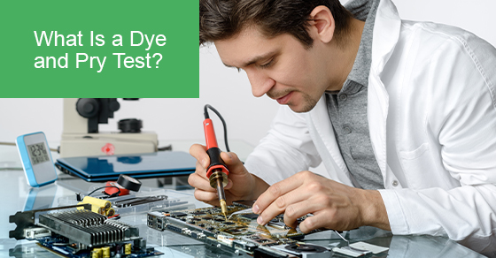
What Is a Dye and Pry Test?
When it comes to putting together your electronics, there’s a whole lot to consider. The design process is one such step, planning exactly how things work and will fit together but equally important is the actual building process. You want both quality and efficiency in your work, hopefully, blended with affordability too, if you can swing it.
However, it’s easy to put together SMT components only to find yourself at a dead end when things don’t work as expected and you end up with glitches or misfiring circuits. This is incredibly frustrating, time-consuming to troubleshoot and it’s often difficult to nail down the exact issue.
However, if you use proper quality soldering and solid quality control methods you can avoid this realm of issues entirely and get to the actual nitty-gritty of using your manufactured goods at their best. To that end, it may be worthwhile to get some dye and pry tests done by experts or even by yourself if you think you can handle it. But that leaves the big question of what exactly such a test is, and why exactly you should bother spending the time and effort to get it done.
What does it do?
The purpose of this process, which is called dye and pry testing, or a dye penetrant test, is to reveal hidden discontinuities beneath any SMT components you have. Of course, this process is unwieldy and sometimes destructive, destroying what you have but giving you benefits.
That hidden advantage is the fact that a dye and pry test is the absolute cost-efficient and cost-effective way of verifying all of your solder connections under BGA and other bottom-terminated SMT packages. It can also work to confirm cracks or leaks on any existing sealed parts.
With all these advantages it’s something you should not overlook even if it seems a bit odd at first.
How It Works
But to fully trust the process you need a deep-level understanding of how it works.
Basically, it takes a sample of the board containing the target feature. You need to excise a decent portion of the board, typically with professional tools like a specialized saw blade engineered for precision cutting of circuit boards. This step is vital because if you don’t use the precise tools you need, you may end up damaging the sample, compromising its integrity and introducing new problems that aren’t reflective of the actual unit in question.
Next, this sample is submersed into a special dye. This dye is of very low viscosity, meaning it’s not thick but rather flows smoothly, like water and silk. This is done inside a vacuum chamber.
Using the capillary action from this chamber you can expect the dye to seep out to every crevice and void, as this process is further enabled and maximized by the massive difference in pressure created by the vacuum section. Once it has been immersed and fully soaked with the dye encompassing and covering every single component of the device, you can move on to the next step.
This requires the use of a moisture removal oven, where it is baked until it is completely dry to the touch. From there we’ll carefully fix it in place in a puller assembler that separates all the components from the board.
Once disassembled, the component parts will be examined in close detail under a strong microscope. It’s at this point where the quality check will kick in, with careful examination for any defects and anomalies that have been introduced by this process.
However, even after doing all this, you may still be considering different methods to check your solders and circuit boards, so next we’ll run down the benefits and limitations of this method of quality control.
Advantages and Disadvantages
The key advantage is that this is the best-known method for identifying solder-joint defects on a BGA device, beating every other method for the exact amount of detection available and its capacity to cover a whole unit with ease and precision.
However, the key downside is that the analysis is destructive. It damages the parts used to the point where you won’t be able to analyze the samples with any other techniques afterwards, requiring you to ride or die with this method or pull out more samples.
Another benefit, however, is that it tests all the joints on a BGA at the same time, speeding up the process and meaning that you can cover a lot of ground at once. It’s also capable of finding fine cracks and cratering that might otherwise be completely invisible, even to powerful x-ray systems.
And it’s a well-used methodology, with tons of documentation and compliance standards available to ensure you’re doing everything to the best practices available. However, it does come with significant complexity if the process didn’t already make that clear. You need an expert who can optimize the sample preparation for accurate and complete analysis.
Closing Thoughts
The dye and pry method is much more exacting than its brute-force name may imply. In fact, it’s a complex process that requires lots of specialized tools and knowledge in order to do it properly and efficiently. However, there are a number of benefits to this well-used method that make the complexity well worth it if you decide this is the path you want to take.
Now that you have a deeper understanding of this topic, and you know all the basics you need to know about a dye and pry test, you may be wondering how to get one done if you’re lacking the professional knowledge and expertise to do it safely and properly. Thankfully you can reach out to us at Circuits Central to help with dye and pry tests in the Toronto area.
If you’d like to know more about dye and pry tests, call Circuits Central at 1-888-602-7264 or through our contact page here.