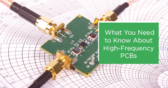
What You Need to Know About High-Frequency PCBs
These days, the employment of high-frequency components and PCBs (printed circuit boards) is becoming increasingly common in technologies used in various sectors. This is largely because of the significant number of advantages that come from using high-frequency PCBs, such as their moderately low costs, their reusability, their long durability, and their compact size.
Electronic circuits tend to behave very differently at higher frequencies, which can pose various problems for a PCB if it is not designed to withstand such frequencies.
The main reason why electronic circuits are affected by higher frequencies is that the behaviour of the passive components, such as resistors, inductors, and capacitors, shifts. Higher frequencies also have a parasitic effect on active components, PCB tracks, and grounding patterns.
The signals between two objects can be disrupted by the noise that high-frequency results in, which requires more energy. However, high-frequency PCBs are manufactured in such a way that they can work at strong frequencies without malfunctioning.
What are the main factors to consider when designing high-frequency PCBs?
It is important that you adopt a different approach when you are designing high-frequency PCBs versus designing PCBs that will not be applied in high-frequency settings. The following are some of the main factors that need to be considered during that process:
1. Choosing the right materials
When PCBs need to operate at high frequencies, it is necessary to make them out of materials that help them support such frequencies. The most important factor is that the materials used to manufacture the board have a low dielectric constant (Dk) and a low dielectric loss tangent (Df).
Dielectrics are insulating materials that can inherently store an electrical charge. Thus, if a material does not have a low dielectric constant, it will store up more electrical charges that will hinder the propagation of the signals, causing propagation delays.
If a material does not have a low dielectric loss tangent, the amount of energy absorbed by the dielectric will increase, resulting in the molecules vibrating at a higher pace, which can also lead to signal loss.
2. Considering thermal management
It is extremely critical to consider thermal management during the design of high-frequency PCBs. As they receive high-frequency signals, the circuit material will eventually begin to generate heat. PCBs have a maximum operating temperature (MOT) at which they can operate. If they exceed this temperature, it threatens their performance and can lead to other side effects like PCB expansion.
The chances of a PCB overheating and malfunctioning can be increased by various factors, such as raised moisture absorption, increased signal crosstalk, and decreased impedance matching.
Fortunately, various thermal management techniques can be applied to high-frequency PCBs, such as the incorporation of via arrays over the copper-filled areas, which allow heat to be dissipated into the air through the vias. The vias should have a large diameter of around 0.1 mm, and the more is used, the better the heat dissipation will be.
Another way to increase heat dissipation is through the use of wider copper traces as well as the use of heatsinks and cooling fans.
3. Multi-layer PCB board wiring
High-frequency circuits typically have both high integration and high wiring density, so it is necessary to use multi-layer boards to reduce interference.
During the PCB layout stage, it should be designed so that a certain number of layers can fully use the intermediate layer to set the shielding, improve the near grounding, effectively reduce the parasitic inductance, and shorten the signal’s transmission length. This can also make a high-frequency PCB more reliable by reducing the signal crosstalk.
4. The leads between the pins
Since the radiant intensity of the signal depends on the length of the trace of the signal line, longer high-frequency signal leads make it easier to couple to the nearby component. Thus, for data, such as signal clock, crystal, and DDR, high-frequency signal lines, like LVDS lines, USB lines, and HDMI lines, must be as short as possible.
It is also better to minimize the transition between the lead layers between the pins of the high-frequency circuit device. Using as few vias as possible is better, as this will significantly increase the speed and reduce the likelihood of data errors.
5. Component placement
Another way to reduce the potential for signal crosstalk is to make the PCB’s circuitry as tight as possible while observing standard design for manufacturability (DFM) rules. It is a good idea to set up component-to-component minimum spacing rules in accordance with manufacturer requirements.
If some parts have different requirements than others due to the assembly process you choose, you can set up specific clearance rules for a group of components and combine these parts into a single component class.
6. Trace routing
Following design rules will make it possible to set up default width and spacing parameters for traces, but you will still need to cover more specific needs by setting up other things.
For example, you should set up individual trace widths and spacings, trace widths and spacings for groups of nets, specific trace widths and spacings for controlled impedance lines, trace width and spacing rules for differential pair routing, and trace lengths and topology patterns for high-speed transmission lines.
It is also crucial to ensure the routing has a clear signal return path that is available on an adjacent reference plane layer and that you do not route any high-frequency lines across splits in the reference plane.
How Circuits Central Can Help With the Design and Production of High-Frequency PCBs
If you have a need for prototype assembly in Toronto, and you require a high-frequency PCB, Circuits Central can provide access to a reliable production facility and a team of experts that are experienced in electronics manufacturing and PCB assembly.
To guarantee that you end up with a high-performing final product, top-notch electronics design and engineering are necessary—and that is exactly what we have to offer. Our engineers can provide an unmatched level of detail during every aspect of the PCB design phase, from schematic diagrams to the PCB layout design.
No matter what stage you are at in designing your PCBs, we are confident that you could greatly benefit from our expertise. Since we have many years of experience in manufacturing PCBs, we are in an optimal position to assist you with the design and layout process. Our team can help you make better technical decisions to limit the chances of experiencing issues down the line. We also employ innovative approaches to PCB design to deliver cutting-edge products.
For more information about our approach to designing and manufacturing high-frequency PCBs or to learn more about our other PCB assembly and manufacturing services, call Circuits Central at 1 (888) 602-7264 or contact us here.