4 Common BGA Rework Mistakes and How to Avoid Them
Ball grid array or BGA rework is one of the most challenging parts of printed circuit board (PCB) assembly and repair. That’s because the BGA is designed to be permanently mounted to the PCB, integrating the circuits. This makes reaching those ball-like pins for repair extremely difficult but not impossible.
A successful BGA rework requires both scientific know-how and an artistic eye. The BGA rework process is well defined online, but it takes a skilled technician to avoid many common mistakes.
Keep reading to see common mistakes made during a BGA rework and how to avoid them. We’ve also added three common defects that can result from these mistakes.
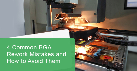
Poor Rework Station
Most DIYers lack the necessary setup to do a correct BGA rework. You’ll need the following as a minimum:
- Adjustable X-Y table to manipulate PCBs during rework
- Temperature-controlled system for soldering paste and PCB heating
- Pressure adjustable suction tool
- Split-beam prism alignment system
- Cameras
- Supplementary software, electronics and components
Compiling all the necessary equipment can equate to a significant investment. Alternatively, you can always get BGA soldering in Toronto done by professionals. We have all of the equipment above, saving you the hassle.
Incorrect Inspection
Solder connections are very hard to see once the connection is complete. It’s especially difficult to see on BGA components because the solder joints are underneath the BGA package.
BGA inspections are carried out to ensure the quality of connections and avoid defects. Unassisted visual inspection simply won’t work here. This is why using the correct BGA inspection option to view solder joints is vital.
Inspection techniques and tools usually fall into one of the following categories.
- Electric- A current is run through the BGA to analyze its stability. Electric inspection is typically done alongside another type as it’s not the best at identifying issue causes.
Optical- While the naked eye is the historical option, medical tools like endoscopes reveal many tiny defects our eyes would miss.
- X-Ray- This is the most advanced inspection option, using x-ray radiation to generate a detailed image. These images are great for identifying variances in solder joint patterns.
Improper Training
Microelectronics manufacturing is a learned skill, not a talent. Often, motivated individuals try BGA reworking after watching a few videos and with no specialized training! This is one of the easiest ways to ensure future issues and defects.
We doubt you want to deal with defects, so take the time to gain hands-on experience in a classroom setting. Remember that even with some training, you’ll likely encounter defects.
Leaving your BGA soldering in Toronto to industry experts like us is the best way to reduce risk and achieve your desired results.
Lack of Preparation
There are a lot of decisions to make before you begin soldering. Choosing a suitable solder paste, and the correct stencils and alloys are all decisions that affect your outcome.
It’s also important to analyze things like solder ball size, solder mask damage and missing or contaminated pads at the PCB site before starting.
Now that you’re familiar with common mistakes people make before starting BGA rework, read on to see three common defects that happen as a result.
Common BGA Defects
Misalignment
When the reflow process changes the positioning of the PCB and BGA, the connection points will not be aligned correctly. This is very common in BGA assembly. BGA components are often light enough to float on molten solder. If too much is used, they can be quickly put out of place. However, when the correct amount of solder is used, they usually stay where you put them, so correct alignment is paramount.
Possible Causes:
- Bad solder application or too much
- A convection rate that is too high
- Excess vibration or rapid speed changes on the conveyor in the reflow oven
- Component oxidization
- Heat sinking of asymmetrical components
How to avoid:
Most of the causes of misalignment can be avoided with some extra attention to detail. Always ensure you are adhering to the recommended temperature and humidity requirements. Try to minimize unnecessary component movement and always place the component in the right spot on pick and place machines. The solderability of the components can be improved by using a more aggressive flux.
Popcorning
Most people are unaware that plastic components like BGAs can absorb moisture from the air. When components absorb humidity and heat is applied, the pressure inside builds, and the steam tries to evaporate. The moisture trying to escape can create a bubble-like effect that damages components known as popcorning.
Possible Causes:
- Packaging not appropriately sealed by the manufacturer
- BGA left outside the package
How to avoid:
Avoiding popcorning damage to your BGA is as easy as keeping it moisture free. Only order moisture-sensitive parts as you require them. This will reduce their chances of just sitting around and sucking up moisture. When you order, look for brands that include a desiccant in the package to keep your BGA dry.
Try baking the moisture out if you suspect your BGA is moisture damaged. Pre-baking before assembly can help prevent cracking in components from popcorning. Just make sure the temperature is below the BGA’s max operating temperature.
Voiding
Voiding describes the empty space or voids that sometimes occur within a solder joint. This is a solder defect because those voids can cause mechanical weaknesses and cracks in the joint. Voiding is common in collapsible BGA components.
Possible Causes:
- Oxidation: Caused by oxidized solder paste
- Low temperature: Preheat temp needs to be high enough that it vaporizes the solvent in the flux
- Too much flux: The flux will not outgas before the solder hardens if too much is used
- Solder paste quality: Some solder pastes shrink in volume when cooled, causing voids and uneven spacing
Design of circuit board- The design and layout of some printed circuit boards (PCBs) make them more susceptible to voiding
How to avoid:
During the preheating phase, preheat for a little bit longer to ensure the ideal temperature is reached. This should increase the likelihood of complete solvent vaporization and prevent leftovers.
You can also try switching solder pastes. As we mentioned above, avoid solder paste that shrinks when cooled like lead-free varieties. Choosing a paste with a lower volatile content can also help reduce voiding. The solder pastes are less likely to draw in moisture from the air, which creates voids. Finally, consider reprinting your PCB. A PCB with gas escape routes to allow for solder paste clearance during reflow is a great design choice.
Call Us
Still not confident in your soldering abilities? We’ve been doing BGA soldering in Toronto for over 25 years, so call us at 1-888-602-7264 or click here to email us.